
HDI Support Multi-Layer PCB Designs
PCB design is a complex process, and high-density interconnect (HDI) technology has streamlined it by increasing routing density on multi-layer boards. This allows designers to make use of smaller components, and enables better signal integrity. HDI also reduces board size and cost. However, it is essential to choose the right materials and layout for your project. Having too many layers in your board may affect its performance and lead to unforeseen costs.
The number of layers in an hdi pcb board depends on the type of stack-up and its height. The layer count should be carefully chosen to suit your application. In addition, the number of vias, microvias and through-holes should also be considered. Smaller vias are more costly and require more precision than larger ones, and adding too many can add up to the overall price of the board.
Using microvias, blind vias, and buried vias in the PCB design reduces board space while maintaining electrical performance. They can also improve signal integrity by reducing the distance between components, which makes them more reliable than traditional through holes. Moreover, the reduced aspect ratio of these vias reduces the distance between the copper layers, which in turn improves impedance control and EMI mitigation.
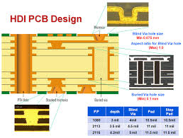
How Does HDI Support Multi-Layer PCB Designs?
Another benefit of HDI is faster time-to-market, since the complexity of the board’s construction allows for more components to be placed in a shorter space. This translates to lower manufacturing costs, as well as higher yields and reliability. Additionally, the reduced aspect ratio of microvias helps improve signal integrity and prevents crosstalk between adjacent traces.
To fabricate a multi-layer HDI circuit board, a special prepreg is used to laminate the various layers together. This is then cooled and stuck to the surface of the board using a hot melt adhesive. This is a key step in ensuring that the board has the correct thickness and electrical performance.
When designing a multi-layer HDI circuit board, the selection of the components is critical. The choice of the component and its placement on the PCB will determine the routing widths, locations, types and sizes of drilled holes, and stack-up. It is essential to understand that these factors will impact the overall performance of the board.
In addition, it is important to consider the thermal management of the circuit board. This is especially important for high-speed signals, which require a large amount of heat. To manage this, the circuit board’s layout must be carefully designed to ensure that the components dissipate heat properly. Lastly, it is essential to pay attention to the layer count and the dielectric thicknesses of the different layers. The layer count will influence the routing speed, and the dielectric thicknesses will influence the maximum feature sizes that can be used.
There are several different ways to create an HDI PCB, including the use of bare copper as the base layer. This will help improve the board’s durability, and is an excellent option for applications in harsh environments, such as avionics and military equipment. Moreover, it can also be utilized in industrial automation, where it is important to be able to monitor and optimize operations.

