

Why Are Blind Vias Important in High-Density PCBs?
Blind Vias Important in High-Density PCBs
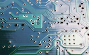
A blind via is a hole that connects an outer layer of a printed circuit board (PCB) to one or more inner layers without penetrating the entire PCB. These vias are not visible on the opposite side of the board, hence the name “blind.” Blind vias are important in high-density PCBs because they allow for more traces and pads to be incorporated into the design without increasing the number of layers or causing excessive stress on the outer surfaces of the board.
In order to use a blind via, the designer must make sure that the drilled hole is filled with copper and that there are pads on the inner surface of the PCB to connect with it. The hole should also be sized correctly; too deep can cause signal distortion and degradation, while too shallow can result in an improper connection.
This can be done using the tools in Altium Designer, but it’s important to talk to your manufacturer before incorporating blind vias into your PCB layout. They will be able to tell you what kind of vias they can fabricate and the maximum possible layers that a blind or buried via can span.
Why Are Blind Vias Important in High-Density PCBs?
Blind and buried vias can be made in two ways: after or before multilayer lamination. In the case of after-lamination, a blind hole is drilled in a core layer or pre-preg material that has been patterned and etched, then copper is plated on the outer surface. The core layer or pre-preg is then stacked together with other layers and pressed to form the finished multilayer PCB.
The other way to produce a blind or buried via is to drill it into the core layers of the PCB during the fabrication process. The holes are plugged with thermal or electrical epoxy and then plated with copper. This can be a more cost-effective solution for high-density PCBs, but it does require an extra processing step that can lead to higher production costs and more potential defects in the board.
Both types of vias are very important for HDI, but it’s important to keep in mind the limitations and costs associated with them. It’s crucial to consult with your manufacturing partner before using these types of vias in your design to avoid costly manufacturing defects.
If you’re ready to get started designing your own high-density PCB, you can try out Altium Designer for free by entering your spec in the online quote calculator. You’ll be able to instantly see the PCB price for your custom spec and receive an accurate shipping quote at checkout. You can also contact us here if you have any questions. We would love to help you find the right circuit board for your project. Best of all, we offer free design assistance on all orders over $100! So what are you waiting for? Click the button below to get your free PCB quote today!